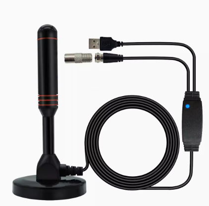
How to Solve Interference with PCB Antennas
Solution to Interference with PCB Antenna
Introduction
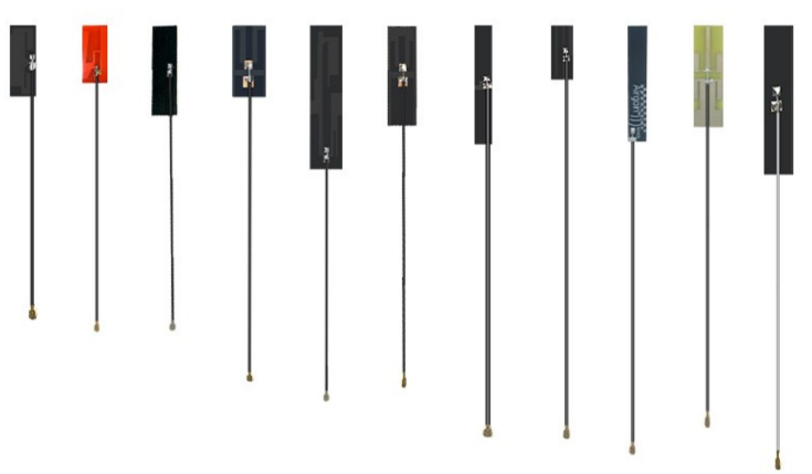
A printed circuit board (PCB) antenna is a type of antenna that is etched onto the PCB, and it is commonly used in electronic devices due to its compact size and ease of integration. However, like any other electronic component, the PCB antenna is susceptible to interference that may lead to poor signal reception or transmission. This article provides solutions to interference issues that may arise in PCB antenna designs.
Potential Sources of Interference
Before delving into the solutions, it is essential to identify the potential sources of interference that can affect the performance of the PCB antenna. Some of the significant sources of interference include:
1. Electromagnetic interference:
This type of interference arises due to the presence of other electromagnetic signals that overlap with the frequency band used by the PCB antenna. The interference can be caused by other wireless devices, such as routers, smartphones, or even other antennas in the same device.
2. Physical obstructions:
Physical obstacles such as metal objects, walls, and even human bodies can interfere with the signal reception of the PCB antenna. This is because these objects can either absorb, reflect or scatter the radio waves, causing signal attenuation.
3. Noise:
Noise in the form of thermal or random signals can also cause interference with the PCB antenna, leading to degraded signals.
Solutions to Interference
To mitigate the effects of interference on the PCB antenna, the following solutions are recommended.
1. Shielding:
One of the most effective ways of reducing interference is to shield the PCB antenna using a metallic shield that can block interfering signals. The shield creates a Faraday cage that prevents electromagnetic waves from entering or leaving the enclosure, hence reducing external interference. However, the shielding material must be carefully selected to avoid signal attenuation caused by resistive losses.
2. Filtering:
The use of filters can also mitigate interference by removing unwanted frequencies from the signal. A filter can either be integrated into the PCB design or added externally to the antenna circuit. The filter can either be passive, such as a simple LC filter, or active, such as a bandpass or bandstop filter.
3. Adjusting the antenna position:
Physical obstructions can be overcome by adjusting the position of the PCB antenna to a location with fewer obstacles that are likely to cause signal attenuation. For example, a higher position with a clear line of sight can improve the reception.
4. Grounding:
Proper grounding of the PCB antenna can help reduce interference by providing a path for the unwanted signals to flow to the ground. The grounding can be achieved by connecting the antenna ground to the device ground plane, which serves as a reference for the antenna.
Conclusion
PCB antennas are a critical component in many wireless electronic devices, but they are susceptible to interference that can reduce their performance. It is essential to identify the sources of interference and adopt effective solutions to mitigate the effects. Shielding, filtering, adjusting antenna position, and grounding are some of the common solutions to interference that can improve the performance of the PCB antenna. By implementing these solutions, the quality of the signal reception and transmission can be significantly enhanced.
